Miller Theorem 6b3427
This document was ed by and they confirmed that they have the permission to share it. If you are author or own the copyright of this book, please report to us by using this report form. Report 3b7i
Overview 3e4r5l
& View Miller Theorem as PDF for free.
More details w3441
- Words: 2,204
- Pages: 5
265
IEEE TRANSACTIONS ON EDUCATION, VOL. 31. NO. 4, NOVEMBER 1988
A Network Theorem Dual to Miller’s Theorem MARIAN K. KAZIMIERCZUK
Abstract-Miller’s theorem is an important tool commonly used in analysis and design of amplifiers with voltage-shunt . A network theorem presented and proved here is dual to Miller’s theorem and can be utilized in the analysis and design of amplifiers with current-series . Three examples are given to illustrate the applicability of the theorem.
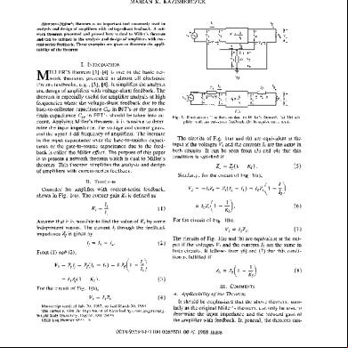
I. INTRODUCTION ILLER’S theorem [1]-[4] is one of the basic network theorems presented in almost all electronic circuits textbooks, e.g., [ 3 ] , [4].It simplifies the analysis and design of amplifiers with voltage-shunt . The theorem is especially useful for amplifier analysis at high frequencies where the voltage-shunt due to the base-to-collector capacitance C,, in BJT’s or the gate-todrain capacitance Cgdin FET’s should be taken into . Applying Miller’s theorem, it is possible to determine the input impedance, the voltage and current gains, and the upper 3 dB frequency of amplifiers. The increase in the input capacitance over the base-to-emitter capacitance or the gate-to-source capacitance due to the is called the Miller effect. The purpose of this paper is to present a network theorem which is dual to Miller’s theorem. This theorem simplifies the analysis and design of amplifiers with current-series .
‘2
‘1
t+ I-
VL
M
(b) Fig. 1. Illustration of the theorem dual to Miller’s theorem. (a) The amplifier with current-series . (b) Its equivalent circuit.
The circuits of Fig. l(a) and (b) are equivalent at the input if the voltages VI and the currents I , are the same in both circuits. It can be seen from (3) and (4) that this condition is satisfied if
Zl = Zf( 1 - K I ) . Similarly, for the circuit of Fig. 1(a),
11. THEOREM Consider the amplifier with current-series , shown in Fig. l(a). The current gain KI is defined as =
Assume that it is possible to find the value of KI by some independent means. The current If through the impedance Zf is given by
From (1) and (2),
v, = ZfIf = Zf(I, =
-
I,)
=
IIZf(1 - K I ) .
(
I,Zf 1
);
*,Zf( 1 -
For the circuit of Fig. l(b),
v, = I,&.
(7) The circuits of Fig. l(a) and (b) are equivalent at the output if the voltages V, and the currents I2 are the same in both circuits. It follows from (6) and (7) that this condition is fulfilled if
z,
=
Zf(1 -
i).
(3)
For the circuit of Fig. l(b),
v, = ZIZ,.
(5)
(4)
Manuscript received July 30, 1987; revised March 30, 1988. The author is with the Department of Electrical Systems Engineering, Wright State University, Dayton, OH 45435. IEEE Log Number 88231 15.
111. COMMENTS A . Applicability of the Theorem It should be emphasized that the above theorem, similarly as the original Miller’s theorem, can only be used to determine the input impedance and the forward gain of the amplifier with . In general, the theorem can-
0018-9359/88/1100-0265$01.OO 0 1988 IEEE
266
IEEE TRANSACTIONS ON EDUCATION. VOL. 31. NO. 4. NOVEMBER 1988
not be applied for calculating the output impedance and the reverse gain. This is because the conditions that exist in the network when K1 is determined are different from those when the output impedance is determined [2], [3]. The mutual equivalence of the circuits shown in Fig. l(a) and (b) is valid only for the forward (from input to output) transmission. Therefore, the output impedance and the reverse gain should be determined from the original circuit of Fig. l(a), using, e.g., a classical nodal or mesh analysis [3] or Blackman’s impedance formula [4].
R, = 2k0
(a)
B. Use@lness of the Theorem In the original Miller’s theorem, an added equivalent impedance, placed in parallel with the load, is [3], [4]
z,=
Zf ~
1
1
(9)
- -
KV
where Kv = V2/ V I . The original Miller’s theorem and its dual version given here are based on the assumptions that it is possible to determine KV or K1 by independent means, respectively. The usefulness-or lack thereof-of Miller’s theorem in either its original or dual version can only be put in proper perspective by evaluating, in any given case, the effect of 1) Z2 on Kv and KV on Z 2 , or 2) Z2 on K, and K I on Z,, whichever applies. The result invokes one of three levels of acceptable approximation. 1) The effect of Z2 on KV or K1 is negligible, in which case one can just ignore it. Then the open-loop gain KV or K1 may be used very conveniently to compute the altered input impedance and the forward gain of the amplifier with . 2) The effect of Z2 on KV or K1 is not negligible, but the effect of KV or K1on Z2 is negligible, the case for large gains (then Z2 = Zr). For acceptable accuracy in using Miller’s theorem to compute the input impedance and the forward gain, one must now include Z2 in computing KV or K1. Although this is a little more trouble, it still leaves Miller’s theorem a viable and insightful approach to getting equivalent input impedance. 3) The effect of KV or K1 on Z, is not negligible and the effect of Z2 on KV or K1 is not negligible either. If Miller’s theorem were now employed, one would be faced with the circular procedure of having to know, say, K1 in order to calculate Z2 in order to calculate K1. In such a case, Miller’s theorem, although still valid, becomes virtually useless. Therefore, a classical nodal or mesh analysis would be advised to get the input impedance and the forward gain.
IV. EXAMPLES A. Example I Fig. 2(a) shows a common-emitter amplifier with current-series . The small-signal parameters of the BJT are h,, = 2.1 kR, hfp = 100, h,, = 0, and h,, = 0. Determine the input impedance R , , the current gain Al =
I(C)
Fig. 2. The common-emitter amplifier with current-series . (a) The circuit. (b) The small-signal model. (c) The equivalent small-signal model.
I n / I s , and the voltage gain A , frequency range.
=
V O / v sfor the midband
B. Solution Fig. 2(b) shows the small-signal model of the amplifier of Fig. 2(a). In this circuit, R,, = R , R 2 / (R I + R , ) = 90 kR, Rf = R,, and the gain K , is
Using the theorem given above, the equivalent circuit of Fig. 2(b) is as shown in Fig. l(c). From ( 5 ) and (8),
RI = Rf(1
-
KI)
=
R,(1
+ h k ) = 101 kR,
The input impedance R,’ is
R , ‘ =v, -=R
I
+ h,, = R , ( 1 + hf,) + h,, = 103.1 kR.
Ib
The input impedance of the amplifier is
The current gain of the amplifier is A1
-
-
In = I,
10 __ 1, Is
=
-h f;r-
RI,
+ R:
-
-46.6.
261
KAZIMIERCZUK: NETWORK THEOREM DUAL TO MILLER'S THEOREM
+l:c
The resistance R2 is connected in series with the ideal current source and therefore does not affect the circuit operation. Since
=5kn
and
the voltage gain is A vs = -Vo= - -Vo=V, V, V, V,
hf,Rc R,(1 + hf,)
I+
Ri
VO
+ hi, Ri + R, 1
Rp = RE(l +-)
R~l1+ hfel
C. Example 2 Fig. 3(a) shows a common-emitter amplifier with the emitter by capacitor. The small-signal parameters of the BJT are hi, = 1 kQ, hf, = 100, h,, = 0 , and h,, = 0. Determine the low 3 dB frequency fL.
-
D. Solution
(C)
Fig. 3(b) shows the small-signal model of the amplifier for the low-frequency range. The current gain KI is
Fig. 3 . Common-emitter amplifier with a by capacitor. (a) The circuit. (b) The small-signal low-frequency model. (c) The equivalent circuit.
where The impedance of the parallel combination of RE and CE in the s domain is
and
1 RE -
RE From ( 5 ) and (8),
SCE 1
+SCE
Fig. 3(c) shows the equivalent circuit of the amplifier. The impedance Z1 is greater than the impedance ZE by a 1 = 101 and consists of the resistance R I factor of hf, in parallel with the capacitance C 1 . Analogously, the impedance Z, is the parallel combination of the resistance R2 = RE( 1 l / h f , ) 2: RE and the capacitance C2 = CE/( 1 + l / h f , ) = CE. However, this impedance does not affect the circuit operation because it is connected in series with the ideal current source. The input impedance of the amplifier is
+
+
Hence, Since
and
IEEE TRANSACTIONS ON EDUCATION. VOL. 31, NO. 4, NOVEMBER 1988
268
where
the voltage gain is
RI
=
1 + hfe +
($
2
and
s
+ W, +
= AV,, ___ s Wp
where the midband voltage gain is
the frequency of the real zero is
+
and the frequency of the real pole is
[
1
+ ”:,l++2’]
=-
f P
Sincefi
=
2 ~ R CE E
<< fp, f L = &
32.4 Hz.
<
WH.
= 32.4 Hz.
ACKNOWLEDGMENT
E. Example 3
KI=
hfe 7
1
+;- W H
where f H = w H / ( 2 a ) = 1 MHz. Determine the impedance Z , for the high-frequency range.
F. Solution From ( 5 ) ,
Thus, the impedance ZI consists of the resistance R I shunted by the capacitance CI. Both R I and C , are functions of frequency. For w / w H = 1 , R I = 100Re = 100 kQ and CI = 1.56 pF; for w / w H = 10, RI = 51.25R, = 51.25 kCl and CI = 1.55 pF; and for w / w H = 100, R I = 2Re = 2 kQ and Cl = 0.79 pF. It can be seen that the resistance R I decreases from Re ( hfe 1 ) to R, as the frequency f increases from zero to infinity. The capacitance CI is very small throughout the entire frequency range and can therefore be neglected. Thus, the advantage of the high input impedance due to the current-series can be fully obtained only for
REFERENCES 111 J . M. Miller, ”Dependence of input impedance of three-electrode vacuum tube upon the load in the plate circuit,” Sri. Papers, Nut. Bureau Stundards, no. 3 5 1 , pp. 362-285, 1919. 121 A. B . Macnee. “On the presentation of Miller’s theorem.” IEEE Trans. Educ., vol. E-28, pp. 92-93, May 1985.
131 A. S . Sedra and K. C. Smith, Microelecrronic Circuits. 2nd ed. New York: Holt, Rinehart and Winston, 1987, pp. 52-56. 141 J . M. Millman and A. Grabel, Mirroc,/ertronics, 2nd ed. McCraw-Hill, 1987, p. 849.
NewYork:
Marian K. Kazimierczuk was born in Poland on March 3, 1948 He received the M S , Ph D , and
-- _ RI
+;wc,
Habilitate Doctorate degrees in electronics engineering from the Department of Electronics, Technical University of Warsaw, Warsaw. Poland, in 1971, 1978, and 1984, respectively In 1972 he ed the Institute of Radio Electronics, Department of Electronics, Technical University of Warsaw. Warsaw, Poland, where he was employed as an Instructor from 1972 and 1978 and as an Assistant Professor from 1978 to 1984 He headed the Radio Electronics Laboratory and the Electronic Apparatus Laboratory from 1978 to 1984. His teaching, research, and development
KAZIMIERCZUK: NETWORK THEOREM DUAL TO MILLER’S THEOREM
269
activities were in the areas of RF power technology, radio transmitters, electronic circuits and systems, semiconductor device modeling, electromagnetic field theory, microwave theory and technique, electronic measurements, circuit theory, communications, and computer-aided design. In 1984 he worked as a Project Engineer at Design Automation, Inc., Lexington, MA, where he was responsible for deg Class E high-efficiency switching-mode dcidc converters. In 1984-1985 he was a Visiting Professor with the Department of Electrical Engineering, Virginia Polytechnic Institute and State University, Blacksburg, where he taught electromagnetic fields and electronic circuits and systems. and his research activity was in the area of power electronics. Since 1985 he has been an Assistant Professor with the Department of Electrical Systems Engineer-
ing, Wright State University, Dayton, OH, where he has been working in the areas of analog and digital electronics, integrated circuits, electronic devices, and power electronics. He is the author of 6 0 scientific papers. of which 19 were published in IEEE TRANSACTIONS and JOURNALS.He also holds six patents related to the new concepts of high-efficiency switchingmode tuned power amplifiers and oscillators. Dr. Kazimierczuk is a member of the Association of Polish Engineers and the Polish Society of Theoretical and Applied Electrical Sciences. He received seven awards from the President of the Technical University of Warsaw, three awards from the Polish Ministry of Science, University Education, and Technology in 1981, 1982, and 1985, and an award from the Polish Academy of Sciences in 1983 for scientific achievements.
IEEE TRANSACTIONS ON EDUCATION, VOL. 31. NO. 4, NOVEMBER 1988
A Network Theorem Dual to Miller’s Theorem MARIAN K. KAZIMIERCZUK
Abstract-Miller’s theorem is an important tool commonly used in analysis and design of amplifiers with voltage-shunt . A network theorem presented and proved here is dual to Miller’s theorem and can be utilized in the analysis and design of amplifiers with current-series . Three examples are given to illustrate the applicability of the theorem.
I. INTRODUCTION ILLER’S theorem [1]-[4] is one of the basic network theorems presented in almost all electronic circuits textbooks, e.g., [ 3 ] , [4].It simplifies the analysis and design of amplifiers with voltage-shunt . The theorem is especially useful for amplifier analysis at high frequencies where the voltage-shunt due to the base-to-collector capacitance C,, in BJT’s or the gate-todrain capacitance Cgdin FET’s should be taken into . Applying Miller’s theorem, it is possible to determine the input impedance, the voltage and current gains, and the upper 3 dB frequency of amplifiers. The increase in the input capacitance over the base-to-emitter capacitance or the gate-to-source capacitance due to the is called the Miller effect. The purpose of this paper is to present a network theorem which is dual to Miller’s theorem. This theorem simplifies the analysis and design of amplifiers with current-series .
‘2
‘1
t+ I-
VL
M
(b) Fig. 1. Illustration of the theorem dual to Miller’s theorem. (a) The amplifier with current-series . (b) Its equivalent circuit.
The circuits of Fig. l(a) and (b) are equivalent at the input if the voltages VI and the currents I , are the same in both circuits. It can be seen from (3) and (4) that this condition is satisfied if
Zl = Zf( 1 - K I ) . Similarly, for the circuit of Fig. 1(a),
11. THEOREM Consider the amplifier with current-series , shown in Fig. l(a). The current gain KI is defined as =
Assume that it is possible to find the value of KI by some independent means. The current If through the impedance Zf is given by
From (1) and (2),
v, = ZfIf = Zf(I, =
-
I,)
=
IIZf(1 - K I ) .
(
I,Zf 1
);
*,Zf( 1 -
For the circuit of Fig. l(b),
v, = I,&.
(7) The circuits of Fig. l(a) and (b) are equivalent at the output if the voltages V, and the currents I2 are the same in both circuits. It follows from (6) and (7) that this condition is fulfilled if
z,
=
Zf(1 -
i).
(3)
For the circuit of Fig. l(b),
v, = ZIZ,.
(5)
(4)
Manuscript received July 30, 1987; revised March 30, 1988. The author is with the Department of Electrical Systems Engineering, Wright State University, Dayton, OH 45435. IEEE Log Number 88231 15.
111. COMMENTS A . Applicability of the Theorem It should be emphasized that the above theorem, similarly as the original Miller’s theorem, can only be used to determine the input impedance and the forward gain of the amplifier with . In general, the theorem can-
0018-9359/88/1100-0265$01.OO 0 1988 IEEE
266
IEEE TRANSACTIONS ON EDUCATION. VOL. 31. NO. 4. NOVEMBER 1988
not be applied for calculating the output impedance and the reverse gain. This is because the conditions that exist in the network when K1 is determined are different from those when the output impedance is determined [2], [3]. The mutual equivalence of the circuits shown in Fig. l(a) and (b) is valid only for the forward (from input to output) transmission. Therefore, the output impedance and the reverse gain should be determined from the original circuit of Fig. l(a), using, e.g., a classical nodal or mesh analysis [3] or Blackman’s impedance formula [4].
R, = 2k0
(a)
B. Use@lness of the Theorem In the original Miller’s theorem, an added equivalent impedance, placed in parallel with the load, is [3], [4]
z,=
Zf ~
1
1
(9)
- -
KV
where Kv = V2/ V I . The original Miller’s theorem and its dual version given here are based on the assumptions that it is possible to determine KV or K1 by independent means, respectively. The usefulness-or lack thereof-of Miller’s theorem in either its original or dual version can only be put in proper perspective by evaluating, in any given case, the effect of 1) Z2 on Kv and KV on Z 2 , or 2) Z2 on K, and K I on Z,, whichever applies. The result invokes one of three levels of acceptable approximation. 1) The effect of Z2 on KV or K1 is negligible, in which case one can just ignore it. Then the open-loop gain KV or K1 may be used very conveniently to compute the altered input impedance and the forward gain of the amplifier with . 2) The effect of Z2 on KV or K1 is not negligible, but the effect of KV or K1on Z2 is negligible, the case for large gains (then Z2 = Zr). For acceptable accuracy in using Miller’s theorem to compute the input impedance and the forward gain, one must now include Z2 in computing KV or K1. Although this is a little more trouble, it still leaves Miller’s theorem a viable and insightful approach to getting equivalent input impedance. 3) The effect of KV or K1 on Z, is not negligible and the effect of Z2 on KV or K1 is not negligible either. If Miller’s theorem were now employed, one would be faced with the circular procedure of having to know, say, K1 in order to calculate Z2 in order to calculate K1. In such a case, Miller’s theorem, although still valid, becomes virtually useless. Therefore, a classical nodal or mesh analysis would be advised to get the input impedance and the forward gain.
IV. EXAMPLES A. Example I Fig. 2(a) shows a common-emitter amplifier with current-series . The small-signal parameters of the BJT are h,, = 2.1 kR, hfp = 100, h,, = 0, and h,, = 0. Determine the input impedance R , , the current gain Al =
I(C)
Fig. 2. The common-emitter amplifier with current-series . (a) The circuit. (b) The small-signal model. (c) The equivalent small-signal model.
I n / I s , and the voltage gain A , frequency range.
=
V O / v sfor the midband
B. Solution Fig. 2(b) shows the small-signal model of the amplifier of Fig. 2(a). In this circuit, R,, = R , R 2 / (R I + R , ) = 90 kR, Rf = R,, and the gain K , is
Using the theorem given above, the equivalent circuit of Fig. 2(b) is as shown in Fig. l(c). From ( 5 ) and (8),
RI = Rf(1
-
KI)
=
R,(1
+ h k ) = 101 kR,
The input impedance R,’ is
R , ‘ =v, -=R
I
+ h,, = R , ( 1 + hf,) + h,, = 103.1 kR.
Ib
The input impedance of the amplifier is
The current gain of the amplifier is A1
-
-
In = I,
10 __ 1, Is
=
-h f;r-
RI,
+ R:
-
-46.6.
261
KAZIMIERCZUK: NETWORK THEOREM DUAL TO MILLER'S THEOREM
+l:c
The resistance R2 is connected in series with the ideal current source and therefore does not affect the circuit operation. Since
=5kn
and
the voltage gain is A vs = -Vo= - -Vo=V, V, V, V,
hf,Rc R,(1 + hf,)
I+
Ri
VO
+ hi, Ri + R, 1
Rp = RE(l +-)
R~l1+ hfel
C. Example 2 Fig. 3(a) shows a common-emitter amplifier with the emitter by capacitor. The small-signal parameters of the BJT are hi, = 1 kQ, hf, = 100, h,, = 0 , and h,, = 0. Determine the low 3 dB frequency fL.
-
D. Solution
(C)
Fig. 3(b) shows the small-signal model of the amplifier for the low-frequency range. The current gain KI is
Fig. 3 . Common-emitter amplifier with a by capacitor. (a) The circuit. (b) The small-signal low-frequency model. (c) The equivalent circuit.
where The impedance of the parallel combination of RE and CE in the s domain is
and
1 RE -
RE From ( 5 ) and (8),
SCE 1
+SCE
Fig. 3(c) shows the equivalent circuit of the amplifier. The impedance Z1 is greater than the impedance ZE by a 1 = 101 and consists of the resistance R I factor of hf, in parallel with the capacitance C 1 . Analogously, the impedance Z, is the parallel combination of the resistance R2 = RE( 1 l / h f , ) 2: RE and the capacitance C2 = CE/( 1 + l / h f , ) = CE. However, this impedance does not affect the circuit operation because it is connected in series with the ideal current source. The input impedance of the amplifier is
+
+
Hence, Since
and
IEEE TRANSACTIONS ON EDUCATION. VOL. 31, NO. 4, NOVEMBER 1988
268
where
the voltage gain is
RI
=
1 + hfe +
($
2
and
s
+ W, +
= AV,, ___ s Wp
where the midband voltage gain is
the frequency of the real zero is
+
and the frequency of the real pole is
[
1
+ ”:,l++2’]
=-
f P
Sincefi
=
2 ~ R CE E
<< fp, f L = &
32.4 Hz.
<
WH.
= 32.4 Hz.
ACKNOWLEDGMENT
E. Example 3
KI=
hfe 7
1
+;- W H
where f H = w H / ( 2 a ) = 1 MHz. Determine the impedance Z , for the high-frequency range.
F. Solution From ( 5 ) ,
Thus, the impedance ZI consists of the resistance R I shunted by the capacitance CI. Both R I and C , are functions of frequency. For w / w H = 1 , R I = 100Re = 100 kQ and CI = 1.56 pF; for w / w H = 10, RI = 51.25R, = 51.25 kCl and CI = 1.55 pF; and for w / w H = 100, R I = 2Re = 2 kQ and Cl = 0.79 pF. It can be seen that the resistance R I decreases from Re ( hfe 1 ) to R, as the frequency f increases from zero to infinity. The capacitance CI is very small throughout the entire frequency range and can therefore be neglected. Thus, the advantage of the high input impedance due to the current-series can be fully obtained only for
REFERENCES 111 J . M. Miller, ”Dependence of input impedance of three-electrode vacuum tube upon the load in the plate circuit,” Sri. Papers, Nut. Bureau Stundards, no. 3 5 1 , pp. 362-285, 1919. 121 A. B . Macnee. “On the presentation of Miller’s theorem.” IEEE Trans. Educ., vol. E-28, pp. 92-93, May 1985.
131 A. S . Sedra and K. C. Smith, Microelecrronic Circuits. 2nd ed. New York: Holt, Rinehart and Winston, 1987, pp. 52-56. 141 J . M. Millman and A. Grabel, Mirroc,/ertronics, 2nd ed. McCraw-Hill, 1987, p. 849.
NewYork:
Marian K. Kazimierczuk was born in Poland on March 3, 1948 He received the M S , Ph D , and
-- _ RI
+;wc,
Habilitate Doctorate degrees in electronics engineering from the Department of Electronics, Technical University of Warsaw, Warsaw. Poland, in 1971, 1978, and 1984, respectively In 1972 he ed the Institute of Radio Electronics, Department of Electronics, Technical University of Warsaw. Warsaw, Poland, where he was employed as an Instructor from 1972 and 1978 and as an Assistant Professor from 1978 to 1984 He headed the Radio Electronics Laboratory and the Electronic Apparatus Laboratory from 1978 to 1984. His teaching, research, and development
KAZIMIERCZUK: NETWORK THEOREM DUAL TO MILLER’S THEOREM
269
activities were in the areas of RF power technology, radio transmitters, electronic circuits and systems, semiconductor device modeling, electromagnetic field theory, microwave theory and technique, electronic measurements, circuit theory, communications, and computer-aided design. In 1984 he worked as a Project Engineer at Design Automation, Inc., Lexington, MA, where he was responsible for deg Class E high-efficiency switching-mode dcidc converters. In 1984-1985 he was a Visiting Professor with the Department of Electrical Engineering, Virginia Polytechnic Institute and State University, Blacksburg, where he taught electromagnetic fields and electronic circuits and systems. and his research activity was in the area of power electronics. Since 1985 he has been an Assistant Professor with the Department of Electrical Systems Engineer-
ing, Wright State University, Dayton, OH, where he has been working in the areas of analog and digital electronics, integrated circuits, electronic devices, and power electronics. He is the author of 6 0 scientific papers. of which 19 were published in IEEE TRANSACTIONS and JOURNALS.He also holds six patents related to the new concepts of high-efficiency switchingmode tuned power amplifiers and oscillators. Dr. Kazimierczuk is a member of the Association of Polish Engineers and the Polish Society of Theoretical and Applied Electrical Sciences. He received seven awards from the President of the Technical University of Warsaw, three awards from the Polish Ministry of Science, University Education, and Technology in 1981, 1982, and 1985, and an award from the Polish Academy of Sciences in 1983 for scientific achievements.
Related Documents 3m3m1z
Miller Theorem 6b3427
December 2019 65
Wilson's Theorem 45152q
December 2019 51
Stokes Theorem 203d68
March 2023 0
Theorem Luroth 19i70
May 2023 0
Black Theorem 31y14
December 2019 43
Hl Theorem 586o46
November 2022 0More Documents from "Siddhant Jain" 4y3j6v
Miller Theorem 6b3427
December 2019 65
Contract Final.doc 692m3u
December 2019 40
Ao Code For Maharashtra 5dg5j
December 2019 62
6l6m1j
April 2020 39
Lets Go Aero Trailers 5o25n
December 2021 0