Point Diode 693v54
This document was ed by and they confirmed that they have the permission to share it. If you are author or own the copyright of this book, please report to us by using this report form. Report 3b7i
Overview 3e4r5l
& View Point Diode as PDF for free.
More details w3441
- Words: 1,019
- Pages: 6
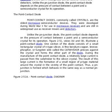
Microwave semiconductor devices. They were developed during World War II for use in microwave receivers and are still in widespread use as receiver mixers and detectors. Unlike the pn-junction diode, the point- diode depends on the pressure of between a point and a semiconductor crystal for its operation. The Point- Diode POINT- DIODES, commonly called CRYSTALS, are the oldest microwave semiconductor devices. They were developed during World War II for use in microwave receivers and are still in widespread use as receiver mixers and detectors. Unlike the pn-junction diode, the point- diode depends on the pressure of between a point and a semiconductor crystal for its operation. Figure 2-51, views (A) and (B), illustrate a point- diode. One section of the diode consists of a small rectangular crystal of n-type silicon. A fine berylium-copper, bronzephosphor, or tungsten wire called the CATWHISKER presses against the crystal and forms the other part of the diode. During the manufacture of the point diode, a relatively large current is ed from the catwhisker to the silicon crystal. The result of this large current is the formation of a small region of p-type material around the crystal in the vicinity of the point . Thus, a pnjunction is formed which behaves in the same way as a normal pnjunction. Figure 2-51A. - Point- diode. DIAGRAM
Figure 2-51B. - Point- diode. P REGION AROUND POINT
Figure 2-51C. - Point- diode. CUT AWAY VIEW
Figure 2-51D. - Point- diode. SCHEMATIC SYMBOL
The pointed wire is used instead of a flat metal plate to produce a high-intensity electric field at the point without using a large external source voltage. It is not possible to apply large voltages across the average semiconductor because of the excessive heating. The end of the catwhisker is one of the terminals of the diode. It has a low-resistance to the external circuit. A flat metal plate on which the crystal is mounted forms the lower of the diode with the external circuit. Both s with the external circuit are low-resistance s. The characteristics of the point- diode under forward and reverse bias are somewhat different from those of the junction diode.
With forward bias, the resistance of the point- diode is higher than that of the junction diode. With reverse bias, the current flow through a point- diode is not as independent of the voltage applied to the crystal as it is in the junction diode. The point- diode has an advantage over the junction diode because the capacitance between the catwhisker and the crystal is less than the capacitance between the two sides of the junction diode. As such, the capacitive reactance existing across the point- diode is higher and the capacitive current that will flow in the circuit at high frequencies is smaller. A cutaway view of the entire point- diode is shown in figure 2-51, view (C). The schematic symbol of a point- diode is shown in view (D). Schottky Barrier Diode: The SCHOTTKY BARRIER DIODE is actually a variation of the point- diode in which the metal semiconductor junction is a surface rather than a point . The large area, or barrier, between the metal and the semiconductor in the Schottky barrier diode provides some advantages over the point diode. Lower forward resistance and lower noise generation are the most important advantages of the Schottky barrier diode. The applications of the Schottky barrier diode are the same as those of the point-diode. The low noise level generated by Schottky diodes makes them especially suitable as microwave receiver detectors and mixers. The Schottky barrier diode is sometimes called the HOTELECTRON or HOT-CARRIER DIODE because the electrons flowing from the semiconductor to the metal have a higher energy level than the electrons in the metal. The effect is the same as it would be if the metal were heated to a higher temperature than normal. Figure 2-52 is an illustration of the construction of a Schottky barrier diode. Figure 2-52. - Schottky-barrier diode.
PIN Diodes The pin diode consists of two narrow, but highly doped, semiconductor regions separated by a thicker, lightly-doped material called the intrinsic region. As suggested in the name, pin, one of the heavily doped regions is p-type material and the other is n-type. The same semiconductor material, usually silicon, is used for all three areas. Silicon is used most often for its power-handling capability and because it provides a highly resistive intrinsic (i) region. The pin diode acts as an ordinary diode at frequencies up to about 100 megahertz, but above this frequency the operational characteristics change. The large intrinsic region increases the transit time of electrons crossing the region. Above 100 megahertz, electrons begin to accumulate in the intrinsic region. The carrier storage in the intrinsic region causes the diode to stop acting as a rectifier and begin acting as a variable resistance. The equivalent circuit of a pin diode at microwave frequencies is shown in figure 2-53, view (A). A resistance versus voltage characteristic curve is shown in view (B). Figure 2-53A. - Diode equivalent circuit (pin).
Figure 2-53B. - Diode equivalent circuit (pin).
When the bias on a pin diode is varied, the microwave resistance changes from a typical value of 6 kilohms under negative bias to about 5 ohms when the bias is positive. Thus when the diode is mounted across a transmission line or waveguide, the loading effect is insignificant while the diode is reverse biased, and the diode presents no interference to power flow. When the diode is forward biased, the resistance drops to approximately 5 ohms and most power is reflected. In other words, the diode acts as
a switch when mounted in parallel with a transmission line or waveguide. Several diodes in parallel can switch power in excess of 150 kilowatts peak. The upper power limit is determined by the ability of the diode to dissipate power. The upper frequency limit is determined by the shunt capacitanceof the pn junction, shown as C1 in figure 2-53, view (A). Pin diodes with upper limit frequencies in excess of 30 gigahertz are available.
Related Documents 3m3m1z
Point Diode 693v54
October 2019 26
Hr Helpdesk Point 241a19
November 2019 97
Point Contours 3s6n4p
March 2021 0
Diode 3i2kf
August 2021 0
Diode Zener 2x1q6v
December 2019 37